 |
J1 And J2 are a matched pair of J310's (can also use U310's or a U431 matched pair). R2 is selected to bias the 2 FETs with a small drain current with no RF input. The turns ratio of the input transformer is selected for an approximate 50 ohm impedance match at the transformer primary (L1).The combined drain current waveform is a rectified sinewave superimposed on a small dc offset (see below). At UHF it is desirable to reduce the drain load impedance and the impedance seen by the JFET sources, thus higher Idss low capacitance JFETs are required. Higher frequency operation is possible if Guanella baluns are substituted for the input and output transformers. N.B. for clarity no parasitic suppression components are shown in the schematic.
 |
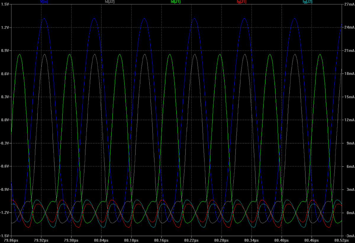
As shown in the (LTSpice) simulated waveforms shown above the drain current waveform is a rectified sinewave with a small dc current superimposed. There is also a small predominantly 2nd harmonic component of drain current flows via the drain gate capacitance of the JFET. This is particularly evident when the source current of each JFET is cutoff. NB the JFETS perform the frequency doubling principally by switching action and not due to the JFET square law input characteristic. The output frequency spectrum of the doubler for a 10MHz +13dBm input as seen at the load is displayed below (reference level is 1V rms). The output level of the frequency doubled component (20MHz)is slightly more than +13dBm.
 |
 |
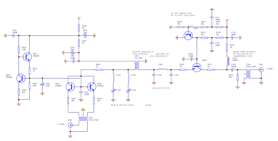
The low phase noise common base BJT frequency doubler shown above is capable of very good performance despite the fact that it uses inexpensive transistors. The low dc gain from base to collector of the dual transistor coupled with the emitter degeneration ensures low phase noise. The circuit is intended for use with 5MHz or 10MHz input frequencies.
Like all frequency doublers it has lowest output phase noise with higher input signals. it is designed for an input of +13dBm and is intended to drive a 50 ohm load (higher load impedances may cause the transistors to enter saturation). The combined collector current waveform is a rectified sinewave superimposed on a small dc offset.Lowest signal phase instability is obtained when a low pass filter with low phase shift at the desired output frequency(2f) is combined with relatively high Q series tuned circuits connected between the common collectors and ground. These tuned circuits suppress the unwanted frequency components in the output (fundamental (f) 3f, 4f etc). The components at f, 3f, 5f etc are due to inevitable transistor and transformer mismatches, however they will have relatively low amplitudes. The high Q series resonant (at f, 3f, 5f etc) tuned circuits will contribute little phase shift and associated instability at the desired 2f output frequency.
 |
The above schematic illustrates filtering the frequency doubler output before feeding the filtered signal to a common base buffer amplifier.
TBC..
Wenzel 2 diode odd-order Frequency Multiplier
Wenzel 4 diode odd order Frequency Multiplier
Wenzel UHF to S band 4 diode odd order Frequency Multiplier